![]()
Technical report
09/2021
Recent progress on the measurement methodology of surface roughness inside the PFA tubes
Hitoshi Imamura
Product R&D Department, Chemicals Division
Daikin Industries, Ltd.
Preface
PFA (tetrafluoroethylene-perfluoroalkyl vinyl ether copolymer) is a perfluoro elastomer-based fluoropolymer that can be melt-processed (1). Its molecular weight is in the hundreds of thousands, and its melt viscosity is 0.01 - 0.1MPa・s (380°C). Various PFA products optimized for compression molding, extrusion molding, injection molding, etc. are commercially available. Due to its excellent purity and chemical resistance, PFA is increasingly in demand as a material for components such as chemical liquid tubes, joints, valves, pumps, filter housings and wafer carriers in semiconductor plants (2) Recently, due to the miniaturization of semiconductor chips, contaminating particles that affect the yield are also nano-sized.
We assume that in order to discuss the possibility of residence of nano-sized particles on the inner surface of PFA tubes, the method for measuring the surface roughness inside the tubes must be newly invented. This paper makes a proposal for a method to measure surface roughness at the nano-level and demonstrate the necessity for this measurement.
Surface roughness of PFA tubes
PFA tubes, which come in contact with high-purity chemical liquids, are pre-washed immediately after installation to remove contaminants adhering to the inner surface. This process is called flushing. Due to the need to reduce the cost and time of this cleaning, the surface roughness of the tubes is one of the targets for improvement.
As the tubes are extruded using the external sizing method, the inner surface crystallizes without touching anything. The outer surface of the tube is water- or air- cooled, but the inner surface is cooled by the air in the tube whose temperature is not well controlled. As a result, the inner surface of the tube has a carapace-like pattern made by spherulites. There used to be some thought that surface roughness could be improved by miniaturizing the spherulites. This theory comes from the appearance of the surface pattern which looks uneven surface.
However, in order for us to understand the nano-sized surface roughness, namely Ra, calculating method from the dimension of spherulite is not appropriate as the scale of those two parameter between the unevenness of the surface and the size of spherulites are different in several digits. It is necessary to discuss nano-sized surface roughness considering the size of lamellar crystals that comprise the spherulite, rather than surface roughness based on the spherulite size.
Fluoropolymers used in this study
1. Material properties
The surface roughness of tubes was evaluated using commercially available PFA listed in Fluoropolymer Handbook compiled by the Japan Fluoropolymer Industry Association (3). The tube was processed by an extruder with a cylinder diameter of 30mmφ using the external sizing method with water-cooling bath. The molding temperature conditions are described in Table 1.
Table.1 Raw material properties evaluated for PFA tubes

2. SEM observation of inner surface of PFA tube
SEM observations were performed as in Fig.1 on PFA1 (NEOFLON PFA SH, manufactured by Daikin Industries, Ltd.) with a spherulite size of ~15µm (15,000 nm) and commercially available PFA2 with spherulite size ~5 µm.
Apparently from visual observation, unevenness of both two tubes made from different material grades are identical in spite of the difference of the size of the spherulites Also, the surface roughness of “on the boundary” and “off the boundary” didn’t show the significant difference. This indicates it is necessary to quantify the unevenness of the “intra-spherulite” rather than that of the “inter-spherulite”. SEM observations of the boundaries between spherulites showed that there were no valleys at the boundary and the boundary area has a surface structure similar to that of the overall spherulite surface, which is also shown in Fig.1.
Fig.1 SEM observation of PFA tube inner surface and spherulite boundary
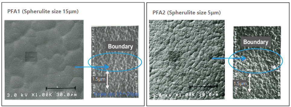
Comment: There is no groove at the boundary. Surface condition equivalent to spherulite surface roughness.
Methods for measuring surface roughness
1. Current method
Conventionally, surface roughness of the inner surface of PFA tubes has been measured by the carapace-like pattern formed by spherulites in the range of evaluation length of 400-4000µm. This method of measuring surface roughness is described in the SEMI standard (F57-0301), JIS standard (B0601) and ISO standard (4287) for semiconductor components. For most cases, the values in the commercial tube for semiconductor application in some catalogs are measured in the same way.
Surface roughness Ra, called arithmetic mean roughness, is calculated as follows: Evaluation length ℓ is extracted from the roughness curve in the direction of the base line, and the absolute values of the deviations from the base line of this extracted portion to the measurement curve are summed and averaged. The calculation formula is shown in Fig.2. By averaging, the effect of a single defect on the measurements can be minimized and stable results can be obtained.
Other general example of the measurement method of the surface roughness on the processed products are a stylus type surface roughness meter and the non-contact laser method. SEMI standard (F57-0301), a representative standard for PFA components for semiconductors, states that the surface roughness of the inner surface of a PFA tube should be Ra ≤ 0.25µm (250 nm). For measurement of the inner surface roughness of a PFA tube, the tube is cut, and its inner surface roughness is measured in the longitudinal direction with a stylus type surface roughness meter. According to the JIS standard (B0601), the ISO standard (4287) and other standards which specify the measurement method for surface roughness, the evaluation length of the roughness curve is determined by the size of surface roughness Ra. A detailed explanation is given in literature (4) in the journal of the Japan Society for Precision Engineering. In the standards, the evaluation length is specified depending on the surface roughness Ra (µm).
If 0.1<Ra≦2, the evaluation length is 4mm. If 0.02<Ra≦0.1, the evaluation length is 1.25mm. Furthermore, if Ra≦0.02, the evaluation length is 0.4mm.
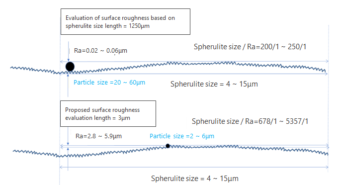
If the evaluation length is 0.4 to 4mm, i.e., 400 to 4000µm, and the spherulite size is 4 to 50µm, the surface roughness Ra can be determined as an unevenness dependent on the spherulite size.
Disadvantage of this measurement method is the fact that the surface roughness Ra is unreasonably underrated if the spherulite size is small. In other words, the method just measures does not measure the unevenness of the small valleys in sub micrometer-scale, but measures the unevenness of the carapace-like pattern which is the macroscopic scale over single µm as surface roughness of the PFA tube’s inner surface. As shown in Fig.1 whether the spherulite size is 5µm or 15µm, the boundaries between spherulites are gently undulating and there is no deep valley.
In observation by an AFM (atomic force microscopy) under similar conditions, it must be noted that the vertical magnification is larger than the reality in order to emphasize the difference of the sample. In Fig.4 in the next section, the spherulites, represented in a 30µm square AFM topographic image, look just like balls. This might have led us to a completely different conclusion from the reality of surface roughness. It is clear from the SEM observation of the spherulite boundaries shown in Fig.1 that the roughness of boundaries between spherulites can be represented by the roughness of spherulite surfaces.
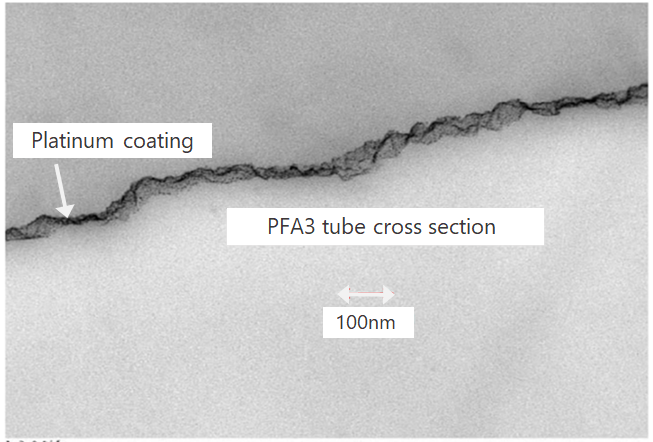
2. TEM observation of PFA tube cross section
Across-section of a 1-inch tube was observed by high acceleration voltage transmission electron microscopy (TEM) using frozen ultrathin sliced piece samples. An example of observation of PFA3 is shown in Fig.3. This cross-sectional TEM image shows that the inner surface of the tube has fine unevenness ranging from a few nanometers to tens of nanometers.
Fig.2 Calculation method of arithmetic average roughness Ra
[ Arithmetic mean roughness Ra ]
Evaluation length ℓ is extracted from the roughness curve in the direction of the average line, and the absolute values of the deviations from the average line of this extracted portion to the measurement curve are summed and averaged.
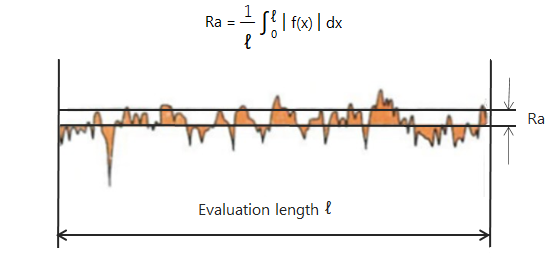
Fig.3 Freezing ultrathin section TEM of cross section of PFA tube
3. Measurement by atomic force microscopy (AFM)
For nano-sized contaminating particles, nano-sized roughness of the spherulite surface must be studied. The author measured the surface roughness of a tube in a 3μm square measurement area, with an evaluation length smaller than the spherulite size, by an AFM under the following conditions. Surface roughness Ra was measured using an AFM5200S (HITACHI High-Tech) large high-precision probe microscope unit, in the dynamic force mode. A measurement area of 3μm of the sample surface was measured with a scanning speed of 1Hz, x-y direction 256×256 division, and cantilever SI-DF-20 (Si, f=134kHz, C=16N/m). The AFM topographic image was calculated by performing an automatic inclination correction process.
Fig.4 shows AFM observation of an area of 30µm square. The horizontal axis of the roughness curve is 29,882nm and the vertical axis is 250nm. Fig.5 shows AFM observation of an area of 3µm square. The horizontal axis of the roughness curve is 2988nm and the vertical axis is 39nm.
In Fig.4, each peak represents a spherulite. It is noted that the ratio of height to width is different from the actual – in Fig.4, the peaks are steeper than they actually are as the vertical scale is magnified by about 20 times.
Meanwhile, as stated in the literature (2), the quality of injection-molded products depends greatly on the surface roughness of the mold metal. There is no carapace-like pattern of spherulites on the surface that has contacted the mold. There is also no spherulite surface on a surface cut by machining. These surfaces are rougher than the inner surface of an extruded tube. The SEMI standard (F57-0301) for the surface roughness of the inner surface of a PFA tube is Ra ≤ 0.25µm, while that for injection molded products is Ra ≤ 0.38μm and that for machined products is Ra ≤ 0.62µm. In these cases, surface roughness may be increased by scratches, and conventional method is suitable as the evaluation method.
But again, in the case of tube application, it is considered from this study that it is necessary to measure the microscopic roughness on the spherulite surface rather than the microscopic surface roughness caused by spherulite size as shown in the previous section
4. Comparison of PFA materials and various surface roughness measurement methods
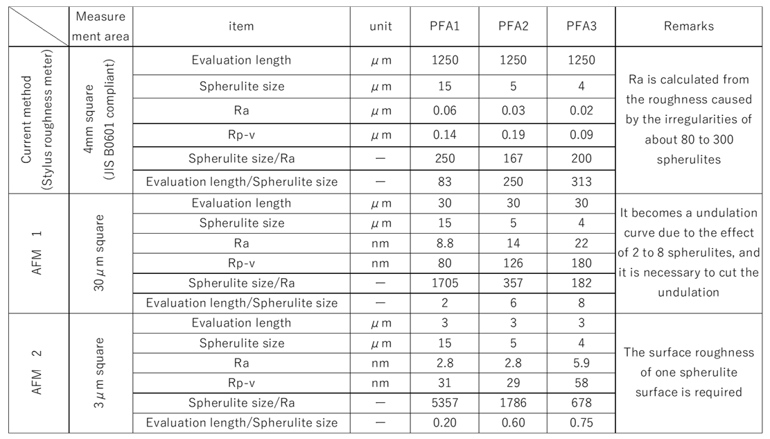
The surface roughness Ra of spherulite surfaces of tubes made with PFA1, PFA2, and PFA3 was compared by AFM. The measurement results are shown in Fig.4, Fig.5, and >Fig.6. Surface roughness measurements of various measurement areas, i.e. different evaluation lengths, are summarized in Table 2. With an evaluation length of 3μm, the results for PFA1 and PFA2 tubes were Ra = 2.8(nm). For PFA3, the result was Ra = 5.9(nm).
Conventionally, discussion on surface roughness assumes that foreign contaminating objects sized 20 to 60nm locates and sticks in the valleys at the boundaries between spherulites. But this is unrealistic as illustrated in Fig.7 if an actual scale were taken into account.
The measurement of roughness of the spherulite surface proposed in this paper is suitable for imagining foreign objects sized 2 to 6nm adhering to uneven surfaces. This is assessed to be a realistic measuring method.
Fig.4 AFM observation of the inner surface of the PFA tube
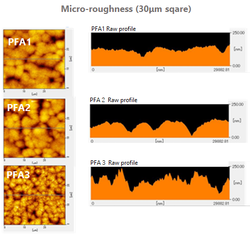
Fig.5 AFM observation of the inner surface of the PFA tube
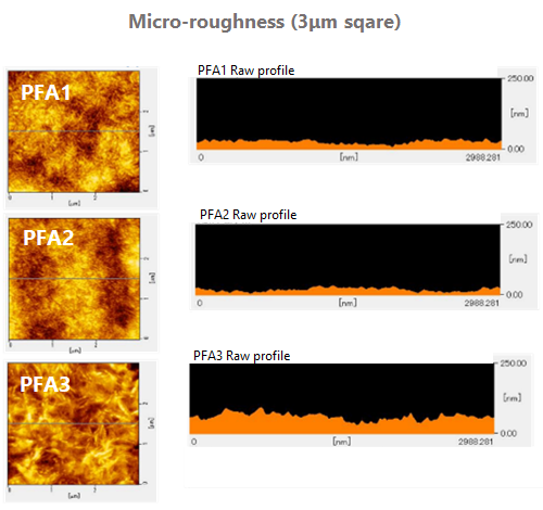
Fig.6 AFM observation of the inner surface of the PFA tube ( 3μm square area )
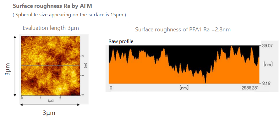
Table.2 Summary of PFA tube surface roughness measurement results>
Note*
1) In the table, Ra represents surface roughness, which is calculated by extracting the evaluation length from the roughness curve and summing and averaging the absolute values of the deviations from the average line of this portion to the measurement curve.
2) Rp-v (or sometimes represented as Ry) is calculated by extracting the evaluation length from the roughness curve and summing Yp from the average line of this portion to the highest peak and Yv to the lowest bottom, i.e. Rp-v = Yp + Yv
Fig.7 Spherulite size and surface roughness image of spherulite surface
5. Analysis of nano-size surface roughness
The unevenness on spherulite surfaces are formed by lamellar bundles, or bundles of lamellar crystals consisting of folded molecular chains. The size of the lamellar bundle is thought to determine the size of the nm-size unevenness (smoothness). PFA is a copolymer of TFE and PAVE and the size of the lamellar bundle may vary depending on the type of PAVE and the amount of nucleating agent, and it has been realized that this leads to variation in nano-level smoothness. Figure 8 shows the result of SEM observation of spherulite surfaces by Elionix ERA-9000.
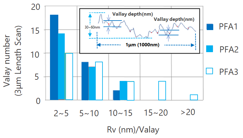
Arithmetic mean roughness Ra is an average value. We applied electron beam three-dimensional roughness using similar equipment and measured the depth and the number of valleys in the evaluation length of 1μm. The results are shown in Fig.9. The proposed method of measuring the roughness of spherulite surface of 3μm square by AFM is considered to make possible discussions of identification/preventive measure of particule issue-, which will be a problem for the next generation of semiconductor chips.
Fig.8 SEM observation of spherulite surface of PFA tube
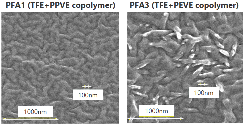
Fig.9 Electron beam three-dimensional roughness analysis
( Releationship between valley depth Rv and valley number )
Conclusion
It has become clear that the current discussion of smoothness based on the current measurement method is unrealistic. SEM observation has revealed that there is no deep valley at the boundaries between spherulites exhibits the similar level of the microscopic unevenness to that on the spherulites. In other words, at the nano level, the surface roughness of the spherulite surface represents the surface roughness of the entire inner surface of the tube.
This paper proposes a method to measure the roughness of the spherulite surface by AFM as a means to measure the surface roughness of PFA tubes, which can meet the needs of miniaturization of semiconductor chips. However, even the latest particle counters has limited capabilities of measuring particles down to 20-30nm in size. Further studies are needed to understand the correlation between the proposed nano-size surface roughness measurement and contaminating and cleaning properties of nano-sized particles.
References
- (1) Takaomi Satokawa, Ed., Fluoropolymer Handbook, Nikkan Kogyo Shimbun (1990), pp. 3-341
- (2) Hitoshi Imamura: Clean Technology, November issue, 5 (2002)
- (3) Japan Fluoropolymer Industry Association, Fluoropolymer Handbook, (revised 13th edition, 2014
- (4) Journal of the Japan Society for Precision Engineering, Vol. 78, No. 4, (2012), pp.301-304
Note** This technical report was originally published in the December 2019 issue of Clean Technology, to which some additions have been made.
Note***All the data shown in this report are not guaranteed.


